Home > Nanotechnology Columns > NanoGlobe > First Asia workshop on Helium Ion Microscope
 |
NanoGlobe Pte Ltd Nanotechnology Business Development Consultants NanoGlobe Pte Ltd |
Abstract:
National University of Singapore (NUS) hosted the 1st Asia workshop on the Helium Ion Microscope (HIM) on 10 September 2009. Seven speakers from NUS, US and Dutch joined this workshop for sharing their experience and insights on using HIM for improving their imaging & fabrication technique. HIM is an emerging powerful instrument for applications in the materials (including bio materials) characterization and fabrication, with the imaging resolution to be as high as 0.24 nm.
November 6th, 2009
First Asia workshop on Helium Ion Microscope
The 1st Asia workshop on the Helium Ion Microscope (HIM) was held on 10 September 2009 in National University of Singapore (NUS). Seven speakers from NUS (Singapore), Carl Zeiss SMT Inc (USA) and TNO (Amsterdam) gave the presentation to share their experience and insights on using HIM for improving their imaging & fabrication technique. Over 100 researchers and students attended this event to learn this new powerful instrument for applications in the materials (including bio materials) characterization and fabrication.
The HIM has been described as an impactful imaging technology. Combining a high brightness ion source with unique sample interaction dynamics, the HIM provides images offering unique contrast and complementary information to existing charged particle imaging instruments such as the SEM and TEM. By scanning the surface with a fine helium beam formed by a single atom at the tip of a 2 metre tall emitter, HIM can produce image resolution as high as 0.24 nanometre, which is the highest recorded resolution for secondary electron imaging. The small interaction volume between the helium beam and the sample also results in images with stunning surface detail. HIM has a five-time high depth of focus (DOF) than that of SEM, which is ideal for the inspection of high-aspect-ratio samples. HIM combines both the high resolution and the high surface sensitivity because of the extremely localized secondary electron (SE) launch location.
Prof. Dan Pickard shared his experience on direct patterning and imaging of grapheme structures with a HIM. Graphene ribbons with 10 nm width and 3.5 �m length can be reliably patterned with HIM, and they can increase the bandgap by changing the width of ribbon grapheme to very narrow size (smaller than 5 nm). However, contamination and substrate effects still remain challenges for the future devices. In addition to the imaging and patterning with HIM, Dr Diederik Maas from TNO, Science & Industry, Amsterdan described another significant applications with the helium ion beam, which is the Helium Ion Beam Lighography (HIBL) and Helium Ion Beam induced deposition (HIBIP). Their scanning HIBL technique can reach the resolution up to 6+/-1nm and 14+/-1nm for the HSQ negative resist and PMMA positive resist, respectively.
To-date, there are only 12 such microscopes in the world, and NUS is the first in Asia to acquire this high-powered microscope.
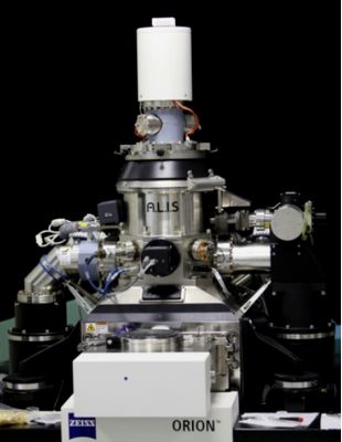 |
| Helium Ion Microscope with sub-nm resolution (0.24nm) |
Bookmark:


|
|
||
|
|
||
| The latest news from around the world, FREE | ||
|
|
||
|
|
||
| Premium Products | ||
|
|
||
|
Only the news you want to read!
Learn More |
||
|
|
||
|
Full-service, expert consulting
Learn More |
||
|
|
||