Home > Nanotechnology Columns > UAlbany College of Nanoscale Science and Engineering > What is lithography?
 |
John G.Hartley CNSE Associate Head of the Nanoengineering Constellation, CNSE Professor of Nanoengineering UAlbany - College of Nanoscale Science & Engineering |
Abstract:
Lithography is a word with two distinct definitions. If you Google "lithography", 7 of the first 10 hits will refer you to the art world and a process invented by Aloys Senefelder in 1788(1). A short description of the process from the Merriam-Webster Online Dictionary defines it as "the process of printing from a plane surface (as a smooth stone or metal plate) on which the image to be printed is ink-receptive and the blank area ink-repellent". This definition belies the major role that the second definition plays in modern society. Again, from Merrian-Webster, we have the second definition: "the process of producing patterns on semiconductor crystals for use as integrated circuits". It is not an understatement to claim that progress in lithography is the engine that has driven much of the world's high-tech economy over the last 50 years.
July 20th, 2009
What is lithography?
Lithography is a word with two distinct definitions. If you Google "lithography", 7 of the first 10 hits will refer you to the art world and a process invented by Aloys Senefelder in 1788(1). A short description of the process from the Merriam-Webster Online Dictionary defines it as "the process of printing from a plane surface (as a smooth stone or metal plate) on which the image to be printed is ink-receptive and the blank area ink-repellent". This definition belies the major role that the second definition plays in modern society. Again, from Merrian-Webster, we have the second definition: "the process of producing patterns on semiconductor crystals for use as integrated circuits". It is not an understatement to claim that progress in lithography is the engine that has driven much of the world's high-tech economy over the last 50 years.
In modern semiconductor manufacturing, the lithographer imposes structure on a beam of light by having it pass through a "mask" followed by projecting the image onto a silicon wafer coated with a thin layer of material called resist (Figure 1). The resist undergoes a chemical transformation when exposed to light. This transformation alters the solubility of the material so that when placed in a developer of an appropriate solvent the latent pattern image transforms into a patterned chemical stencil. This chemical stencil then serves as the template for further process steps. Deposition and etching tools add or remove material as needed through the openings in the chemical stencil. Another process step strips away the chemical stencil and a fresh layer of resist is applied. The process repeats until all of the device levels necessary to build a full device have been assembled. The enormous productivity of modern electronics is driven by the capability of a single lithographic machine to pattern features at a rate in excess of 100 trillion features per hour. To help put this in context, if dollars were printed at this rate, it would take about 7 minutes to pay of the US national debt (2009).
Modern lithographic equipment operates well inside the nanoscale regime, defined as features smaller than 100 nanometers (nm). The College of Nanoscale Science and Engineering (CNSE) is home to numerous systems of this caliber. The light bulb in Figure 1 is intentionally shown as blue. The reason has to do with the wavelength of light - the bluer the light, the shorter its wavelength and the smaller the features that can be imaged. Visible light ranges from a wavelength of 700nm at the red end of the spectrum to 400nm at the violet. Beyond violet in the visible light spectrum, one finds the ultraviolet light familiar from sunburn. The lithography systems shown in Figure 2 (a-c) operate in the Deep Ultra Violet (DUV) portion of the spectrum at a wavelength of 193nm and print features as small as 90nm for the 1st generation system (a) to 45nm for the 3rd generation machine (c). To go to even smaller features, the operating wavelength of the light source must shift even further to the blue, dropping to 13.5nm in the Extreme Ultra Violet (EUV) portion of the spectrum (d). At this wavelength, air absorbs the light so strongly that it is necessary to carry out lithography in a vacuum.
Photons are not the only means of exposing resist for image formation. Electrons have been used for this purpose as well for nearly 50 years(2). Electrons have the advantage of being easily controlled electronically and they enable the most direct means of translating a pattern from the designers computer file to a latent image in resist. They are also capable of forming images of incredibly high resolution, with 10nm being fairly routine and smaller features achievable with some effort. The electron beam lithography system at CNSE is shown in Figure 3(a). It is capable of patterning both directly on wafers as well as the substrates used for masks in the optical lithography tools.
Closest to the original spirit of lithography is the Molecular Imprints nanoimprint system at CNSE under the International Sematech program (Figure 3b). Rather that using projected photons or electrons to form a pattern, this system works by displacement of a very thin fluid layer on the wafer with a proximity contact mold. While the fluid is displaced by the mold, it is flashed by a short burst of UV radiation which cures the fluid. The mold pulls away leaving the pattern behind and moves on to repeat the process for the next copy. This technology is capable of the same resolution as electron beam lithography and is frequently limited by the quality of the mold fabrication process.
All of the lithographic techniques described here form the basis of what is known as "top down" patterning. The materials patterned are essentially "dumb". All of the pattern data is imposed on the material from the outside. The other means of patterning under investigation by nanotechnologists is "bottom up", where the intelligence to build the pattern is built into smart materials that self assemble into complex structures. If you doubt that such a thing is possible, you only need to look into a mirror to see a working proof of concept. Taking control of an arbitrary design, however, is very much work in progress - stay tuned�
1. "lithography." Britannica Concise Encyclopedia. 2005. Encyclop�dia Britannica Premium Service 14 Feb. 2005 http://www.britannica.com/ebc/article?tocId=9370361
2. G. Mollenstedt and R. Speidel, Physik. Blatter 16, 100 (1960).
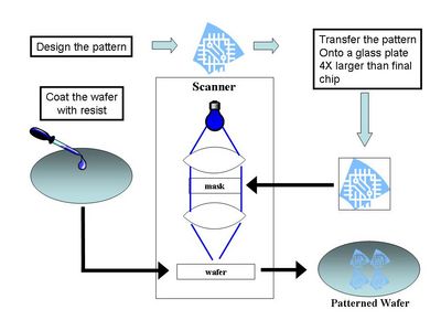 |
| Figure 1: Basic illustration of the lithographic process used in modern nanoscale semiconductor manufacturing. |
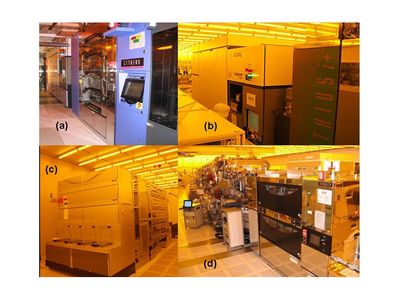 |
| Figure 2: Four of the CNSE photon based lithography tools built by ASML with resist tracks from Tokyo Electron. (a) � (c) are 3 generations of 193nm DUV, water immersion systems while (d) uses 13.5nm EUV photons. |
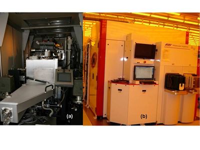 |
| Figure 3: Two non-photon based lithography systems at CNSE. (a) Vistec VB300 electron beam system. (b) Molecular Imprints Imprio 300 nanoimprint system. |
Dr. John Hartley's bio: http://cnse.albany.edu/StaffDirectory/index.cfm?InstanceID=576&step=staffdetail&StaffDirectoryID=16
Bookmark:


|
|
||
|
|
||
| The latest news from around the world, FREE | ||
|
|
||
|
|
||
| Premium Products | ||
|
|
||
|
Only the news you want to read!
Learn More |
||
|
|
||
|
Full-service, expert consulting
Learn More |
||
|
|
||